
specialists in PCB Design & Fabrication
Bringing you state-of-the-art boards at affordable prices, we pride ourselves in providing you with viable solutions to your needs through our years of expertise and skills
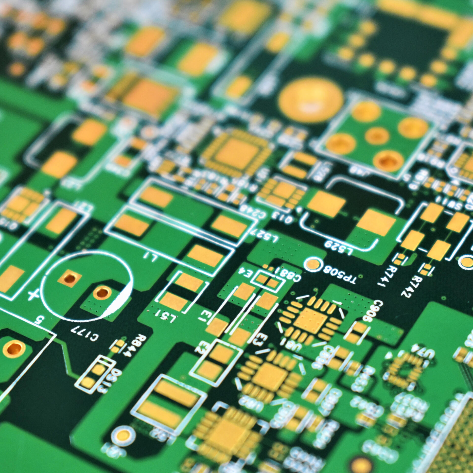
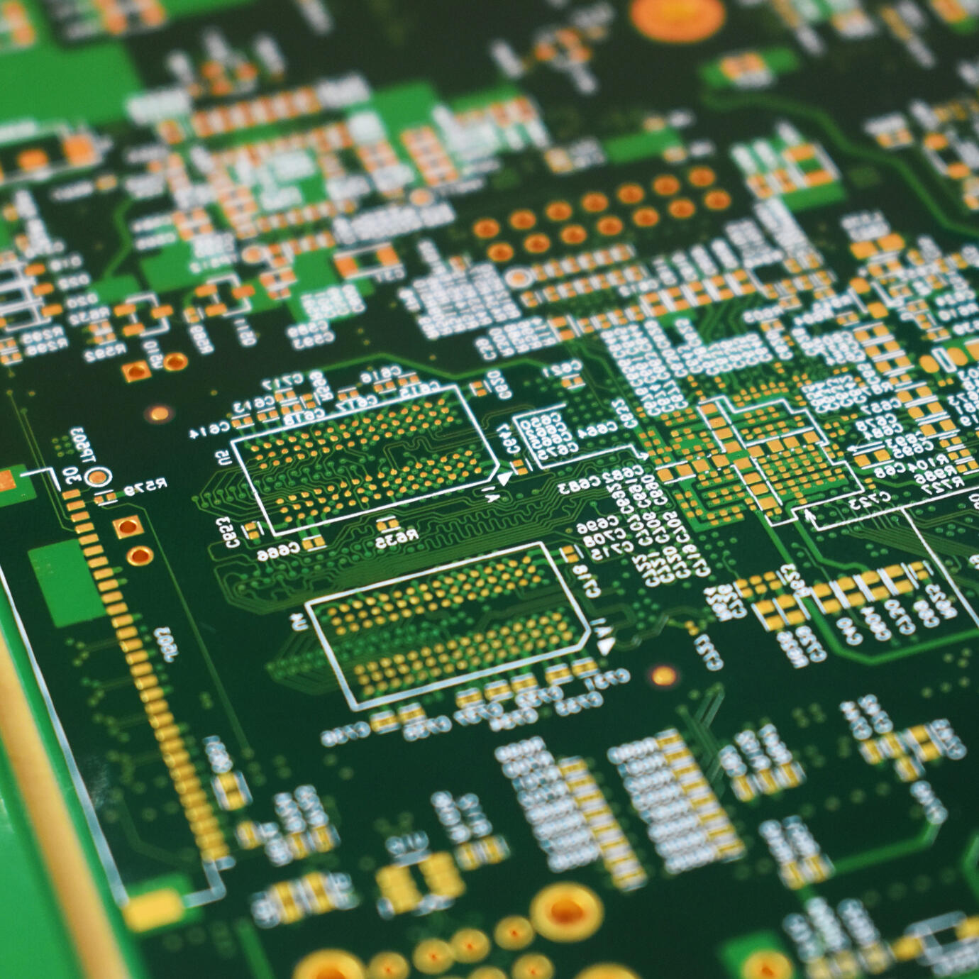
About Us
Through reliable work flows, we believe in maintaining consistent communication between our customers in order to constantly review on the design for maximum customer satisfaction. All Gerber files are also generated and reviewed by us to reduce front-end queries from PCB manufacturers.We also work closely with our PCB vendor and assembly house for PCBA.
Our philosophy
We believe in doing everything right the first time and everytime.With our services, we can promise the following.
Experience
Analog, RF, high speed design, you name it, we have it. Your project will be realized from conceptualization to production.
Affordable
Realizing your project will not only of high quality but also cost-effective.
Efficient
Being efficient is part of our ingrained characteristic. When we promise you a delivery date, you will get it.
Reliable
We pride ourselves on our contactability and friendliness throughout our service.
We believe in our people
for they make us who we are todayFurther your career with us today.
Career
In today's marketplace, applications for the new technology and electronics produced are limitless.Here, we serve to deliver the PCB suited for our customer's needs and demands. Find out how we make this happen and what career opportunities could be there for you!
PCB Assistant
/Design Engineer
Our ideal fit is someone who are proactive and has a high motivation to learn.Further your career with us today.
Description
Overview
As a PCB Assistant/Design engineer, you will be responsible in performing PCB design from schematic capture, footprint creation, placement, routing to Gerber generation. Other job responsibilities will also include creating design documents such as entry schematics and library creations. BOM preparation and parts sourcing are also included.Requirements
Fresh graduates from ITE, polytechnic and university level are welcome.Some behavioural competencies we are looking out for in our candidates include ability to be organized and methodical.Additional details
As training will be provided, no prior knowledge in PCB design is required.Interested?
Email your CV to us at [email protected] and we will get back to you as soon as possible.
services

PCB Design
We will also provide complete assembly drawing and professional fabrication documents.
| Design Tools |
|---|
| Mentor Graphics - PADS |
| Mentor Graphics - PADS Professional |
| Mentor Graphics - Expedition |
| Altium Designer |
| Cadence Orcad |
| Camtastic 2000 |
| Design Capabilities |
|---|
| High-Power Analog Design |
| High-Speed Design |
| High-Density Design |
| RF Design |
| RF Mixed Digital Design |
| HDI Technology - Blind Via, Back Drill Design |
| Embedded Design |
| EMI/EMC Compliance |
| Rigid PCB Design, Rigid Flex, Flex PCB Design |
| IPC Class 2 & 3 Compliance |
| In-Circuit Test (ICT) Data Generation |
| Panel Design |
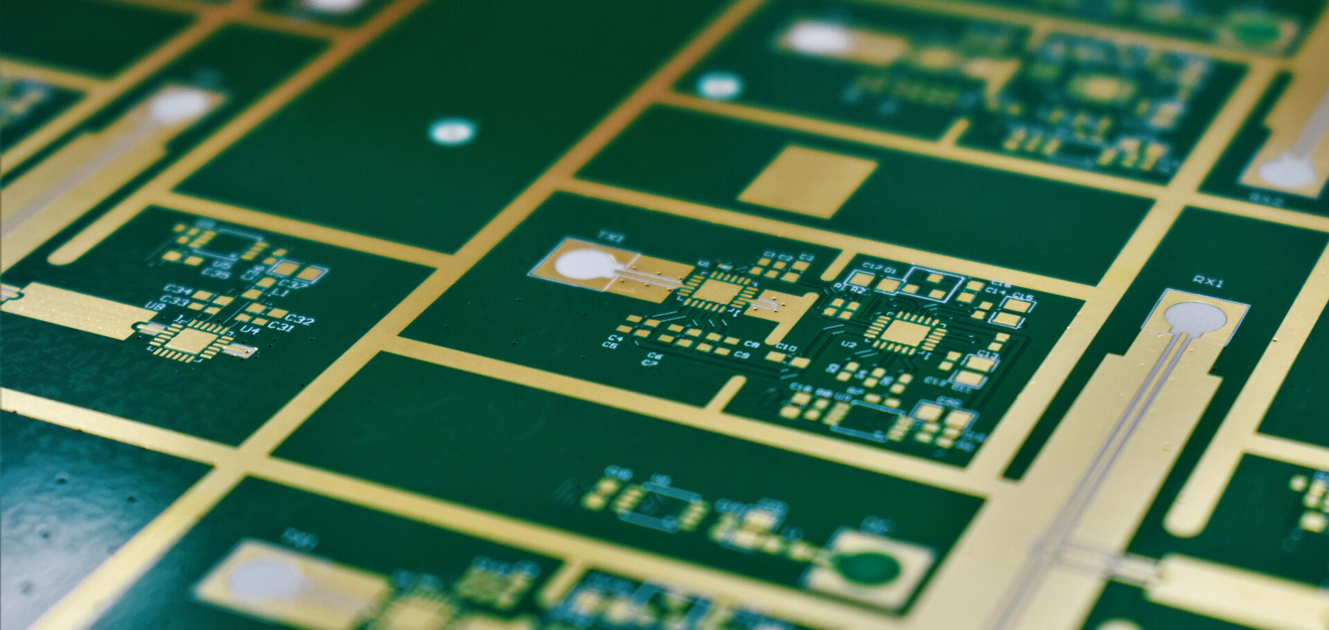
PCB Fabrication
| Item | Sample | Mass Production |
|---|---|---|
| Layer Count | 1 - 56L | 1 - 46L |
| Board Thickness | 0.2 - 10.0mm | 0.4 - 6.0mm |
| Max Board Size | 610 * 1200mm | 710 * 1200mm |
| Copper Weight (UL Approved) | 0.5oz - 0.6oz | 0.5oz - 0.6oz |
| Min Line Width/Space | 3mil/3mil | 3mil/3mil |
| Min Finished Hole size | 0.1mm | 0.15mm |
| Aspect Ratio | 16:1 | 12:1 |
| Impedance Control | +/- 10% | +/- 10% |
| Item | Sample and Mass Production |
|---|---|
| Material Type | FR-4, Rogers, Arlon, Panasonic, Taconic, TUC, Bergquist, Dupont, AIN, AIO, etc |
| Surface Finish | ENIG, ENEPIG, HASL LF, OSP, Hard gold plating, Immersion Tin, Immersion silver, etc |
| Special Technology | Blind & buried vias, Via in pad, hybrid, countsink hole, semi-hole plating, edge plating, step mounting hole, back drill, controlled depth hole, 1+N+1 HDI, gold fingers, etc |
System Certificated
ISO9001:2000
ISO14001:2004
TS16949:2009Product Certificated
UL Certification:E30759ROHS
SGS +REACHManufacturing Standards
IPC-A-600G
IPC-6012B-Class 2

PCB Assembly
Auto Insert Machine (Full SMD Line)
Manual soldering and board rework/repair
CSP and BGA @ 0.3mm pitchIPC Standards: Class 2, Class 3, J-STD-001, A-610, A-620, A-600 and 7711/21
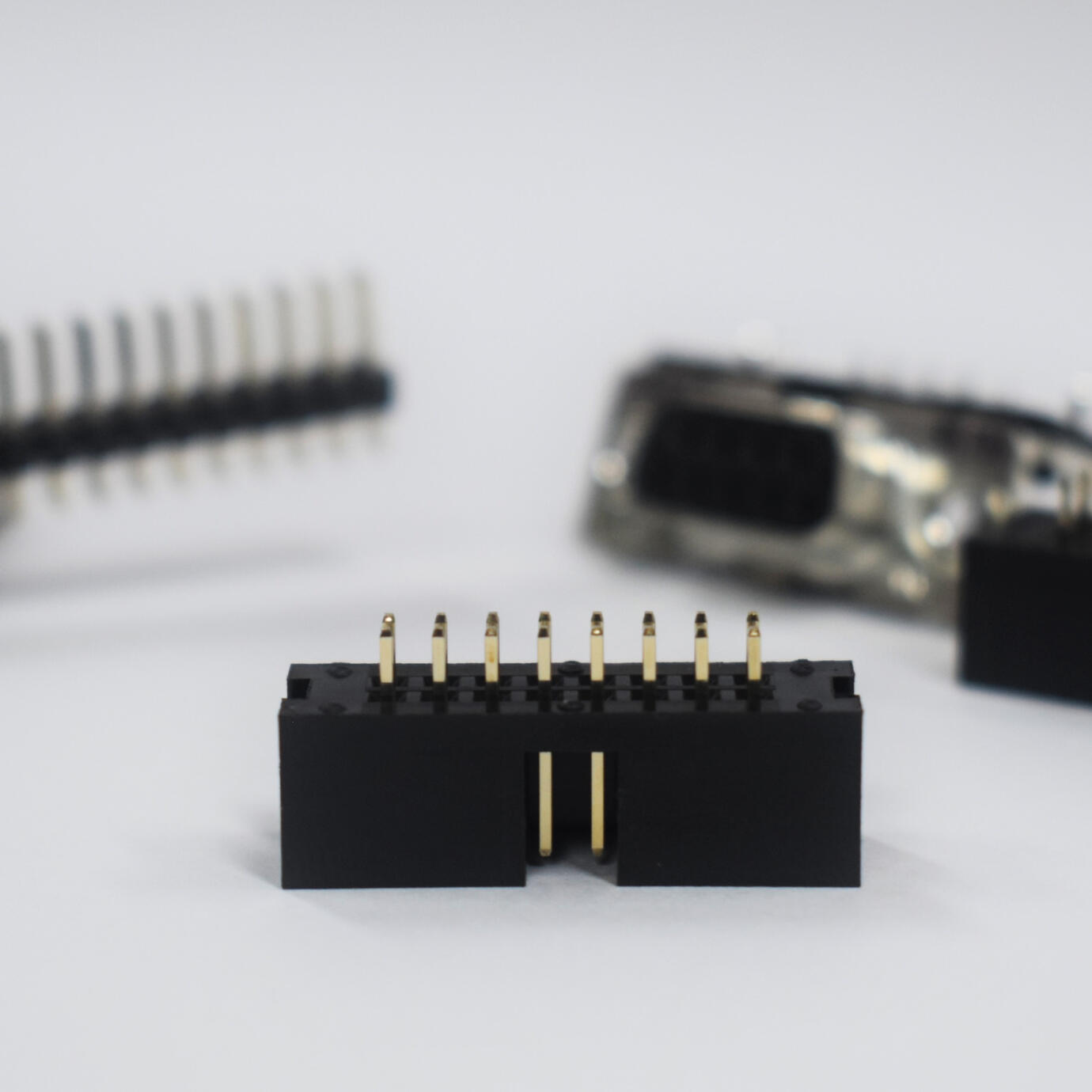
Component Kitting
As we work closely with our distributors, we are able to provide for extensive prototyping needs, from small to mid volume production. Your entire fabrication process will not be daunting anymore with our steady support.
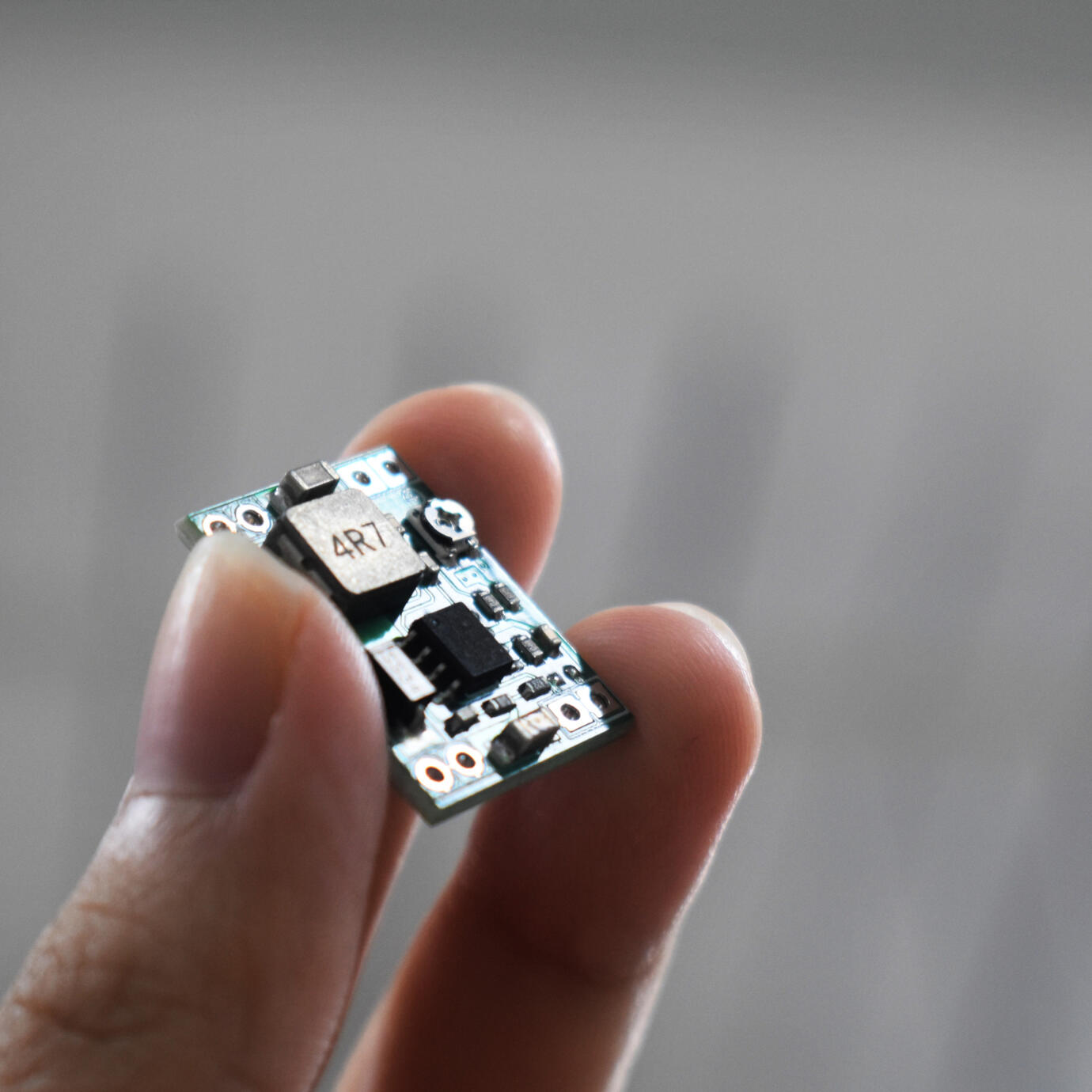
Full Turn-key
Looking for a one-stop solution?From schematics design, placement, routing to gerber checking, PCB assembly is safe in our hands. Likewise, fabrication, components kitting and assembly will be covered by us too. Let us know your idea and we will conceive it accordingly.
Find us
2 Cleantech Loop, #04-05, Singapore 648751[email protected]+65 9741 6002
Get in touch
Anything else that you are unsure of or cannot find on the website?Don't be afraid to reach out to us - we don't bite.
Thank you
It is good to hear from you.
We will keep in touch with you shortly!